You may have designed many PCBs, but you may not know the flow of PCB processing
- Author:
- Source:
- Date : 2023-06-08
You may have designed many PCBs, but you may not know the flow of PCB processing.
Flow of PCB processing and manufacturing.
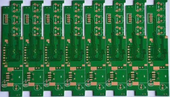
1. CUT
Cutting is the process of cutting the original copper clad laminate into boards that can be made on the production line
First, let's understand a few concepts:
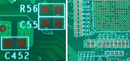
(1) UNIT: Refers to the unit graphics designed by PCB design engineers.
(2) SET: Refers to an overall graphic that engineers put together multiple UNITs in order to improve production efficiency and facilitate production. That is what we often call jigsaw, which includes unit graphics, process edges and so on.
(3) PANEL: Refers to a board composed of multiple SETs combined with tool board edges for reasons such as improving efficiency and facilitating production when PCB manufacturers produce.
2. INNER DRY FILM
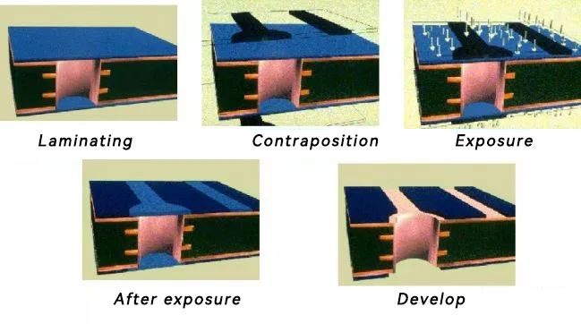
The inner dry film is the process of transferring the inner layer circuit pattern to the PCB board.
In PCB production, we will mention the concept of graphics transfer, because the production of conductive graphics is the foundation of PCB production. Therefore, the graphics transfer process is of great significance to PCB production.
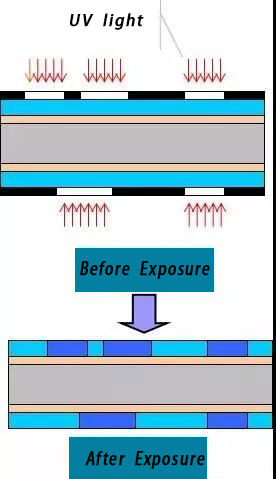
The inner dry film includes multiple processes such as inner film sticking, exposure and development, and inner etching. The inner film sticking is to paste a special photosensitive film on the surface of the copper plate, which is what we call a dry film. This film will cure when exposed to light, forming a protective film on the board. Exposure and development is to expose the plate with the film attached, the part that is transparent is cured, and the part that is not transparent is still a dry film. Then after development, the uncured dry film is removed, and the plate with the cured protective film is etched. After the film is removed, the circuit pattern of the inner layer is transferred to the board. The whole process flow is shown in the figure below.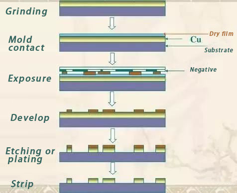 For designers, the most important thing we consider is the minimum line width of wiring, the control of spacing and the uniformity of wiring. If the spacing is too small, it will cause film clamping, and the film cannot be completely removed, which will cause a short circuit. If the line width is too small, the adhesion of the film is insufficient, resulting in an open circuit. Therefore, the safe spacing of production must be considered for safe spacing during circuit design (including line and line, line and pad, pad and pad, line and copper surface, etc.).
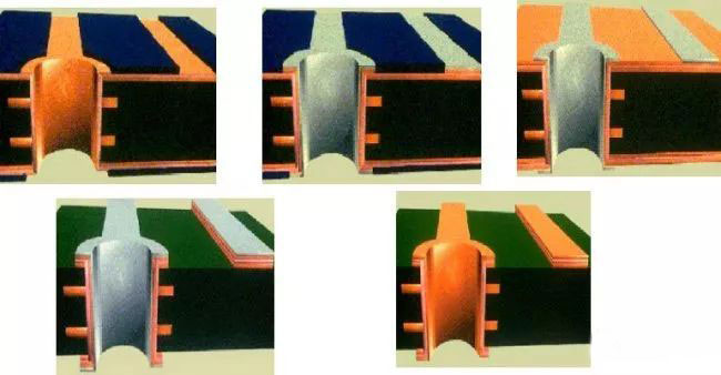
(1) Pretreatment: grinding plate
The main function of grinding plate: The basic pretreatment is mainly to solve the problems of surface cleanliness and surface roughness, remove oxidation, increase the roughness of the copper surface, and facilitate the film to adhere to the copper surface.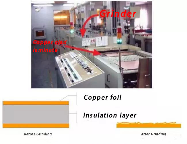 (2) Film pasting
Paste dry film or wet film on the treated substrate by hot pressing or coating to facilitate subsequent exposure production.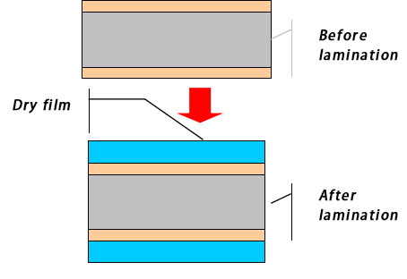 (3) Exposure
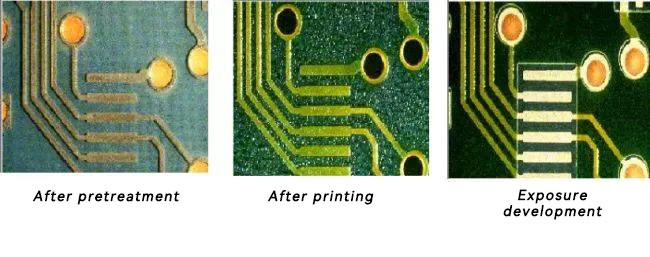
Align the negative film with the substrate on which the dry film is pressed, and transfer the negative film pattern to the photosensitive dry film by irradiating with ultraviolet light on the exposure machine.
Physical picture of negative film
 (4) Development
Use the weak alkalinity of the developer (sodium carbonate) to dissolve and rinse the unexposed dry film/wet film, and keep the exposed part.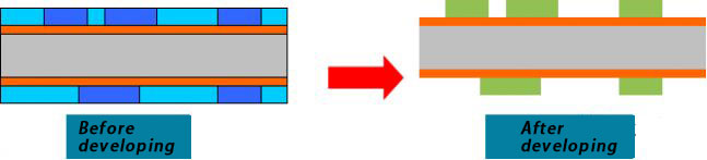 (5) Etching
After the unexposed dry film/wet film is removed by the developer, the copper surface will be exposed, and the exposed copper surface will be dissolved and corroded with acidic copper chloride to obtain the desired circuit.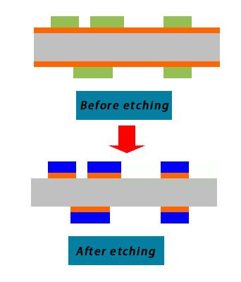 (6) Film removing
Peel off the exposed dry film protecting the copper surface with sodium hydroxide solution to expose the circuit pattern.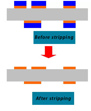 3. Browning
Purpose: To form a microscopic roughness and an organic metal layer on the inner copper surface to enhance the adhesion between layers.
Principle:
A uniform organic metal layer structure with good adhesion characteristics is produced by chemical treatment, which makes the surface of the copper layer roughened before the inner layer is bonded, and is used to enhance the bonding strength between the inner copper layer and the prepreg after pressing.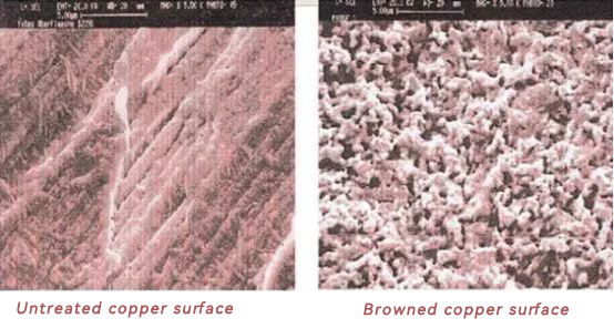
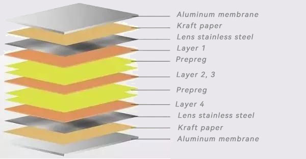
4. Lamination
Lamination is the process of bonding the various layers of circuits into a whole by means of the adhesiveness of the pp sheets. This bonding is achieved through mutual diffusion and penetration of macromolecules on the interface, and then interweaving, and the discrete multilayer boards and pp sheets are pressed together to form a multilayer board with the required number of layers and thickness. In actual operation, copper foil, bonding sheet (prepreg), inner layer board, stainless steel, isolation board, kraft paper, outer layer steel plate and other materials are laminated according to the process requirements.
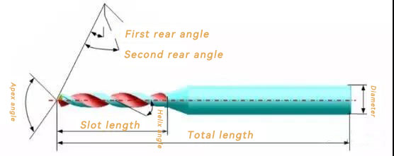
The legendary drilling tool
Flow of PCB processing and manufacturing.
1. CUT
Cutting is the process of cutting the original copper clad laminate into boards that can be made on the production line
First, let's understand a few concepts:
(1) UNIT: Refers to the unit graphics designed by PCB design engineers.
(2) SET: Refers to an overall graphic that engineers put together multiple UNITs in order to improve production efficiency and facilitate production. That is what we often call jigsaw, which includes unit graphics, process edges and so on.
(3) PANEL: Refers to a board composed of multiple SETs combined with tool board edges for reasons such as improving efficiency and facilitating production when PCB manufacturers produce.
2. INNER DRY FILM
The inner dry film is the process of transferring the inner layer circuit pattern to the PCB board.
In PCB production, we will mention the concept of graphics transfer, because the production of conductive graphics is the foundation of PCB production. Therefore, the graphics transfer process is of great significance to PCB production.
The inner dry film includes multiple processes such as inner film sticking, exposure and development, and inner etching. The inner film sticking is to paste a special photosensitive film on the surface of the copper plate, which is what we call a dry film. This film will cure when exposed to light, forming a protective film on the board. Exposure and development is to expose the plate with the film attached, the part that is transparent is cured, and the part that is not transparent is still a dry film. Then after development, the uncured dry film is removed, and the plate with the cured protective film is etched. After the film is removed, the circuit pattern of the inner layer is transferred to the board. The whole process flow is shown in the figure below.
(1) Pretreatment: grinding plate
The main function of grinding plate: The basic pretreatment is mainly to solve the problems of surface cleanliness and surface roughness, remove oxidation, increase the roughness of the copper surface, and facilitate the film to adhere to the copper surface.
Paste dry film or wet film on the treated substrate by hot pressing or coating to facilitate subsequent exposure production.
Align the negative film with the substrate on which the dry film is pressed, and transfer the negative film pattern to the photosensitive dry film by irradiating with ultraviolet light on the exposure machine.
Physical picture of negative film
Use the weak alkalinity of the developer (sodium carbonate) to dissolve and rinse the unexposed dry film/wet film, and keep the exposed part.
After the unexposed dry film/wet film is removed by the developer, the copper surface will be exposed, and the exposed copper surface will be dissolved and corroded with acidic copper chloride to obtain the desired circuit.
Peel off the exposed dry film protecting the copper surface with sodium hydroxide solution to expose the circuit pattern.
Purpose: To form a microscopic roughness and an organic metal layer on the inner copper surface to enhance the adhesion between layers.
Principle:
A uniform organic metal layer structure with good adhesion characteristics is produced by chemical treatment, which makes the surface of the copper layer roughened before the inner layer is bonded, and is used to enhance the bonding strength between the inner copper layer and the prepreg after pressing.
4. Lamination
Lamination is the process of bonding the various layers of circuits into a whole by means of the adhesiveness of the pp sheets. This bonding is achieved through mutual diffusion and penetration of macromolecules on the interface, and then interweaving, and the discrete multilayer boards and pp sheets are pressed together to form a multilayer board with the required number of layers and thickness. In actual operation, copper foil, bonding sheet (prepreg), inner layer board, stainless steel, isolation board, kraft paper, outer layer steel plate and other materials are laminated according to the process requirements.
For designers, the first thing that needs to be considered in lamination is symmetry. Because the board will be affected by pressure and temperature during the lamination process, there will still be stress in the board after the lamination is completed. Therefore, if the two sides of the laminated board are uneven, the stress on the two sides will be different, causing the board to bend to one side, which greatly affects the performance of the PCB.
In addition, even on the same plane, if the distribution of copper is uneven, the flow rate of the resin at each point will be different, so that the place with less copper will be slightly thinner, and the place with more copper will be slightly thicker.
In order to avoid these problems, factors such as the uniformity of copper distribution, the symmetry of the lamination, the design and layout of blind buried holes must be considered in detail during the design.
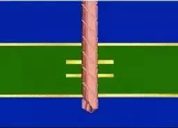
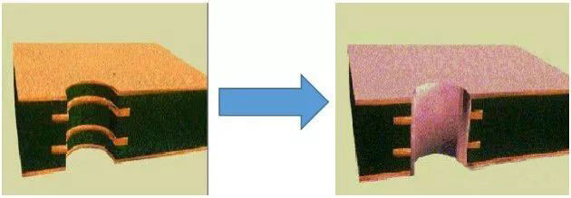
5. Drilling
Through holes are formed between the layers of the circuit board to achieve the purpose of connecting the layers.
In addition, even on the same plane, if the distribution of copper is uneven, the flow rate of the resin at each point will be different, so that the place with less copper will be slightly thinner, and the place with more copper will be slightly thicker.
In order to avoid these problems, factors such as the uniformity of copper distribution, the symmetry of the lamination, the design and layout of blind buried holes must be considered in detail during the design.
5. Drilling
Through holes are formed between the layers of the circuit board to achieve the purpose of connecting the layers.
The legendary drilling tool
6. Immersion copper plating
(1) Immersion copper
Also called chemical copper, the PCB board after drilling undergoes oxidation-reduction reaction in the copper sinking cylinder to form a copper layer to metallize the holes, so that copper is deposited on the surface of the original insulating substrate to achieve electrical communication between layers.
(2) Plate plating
Thicken the surface of the PCB and the copper in the hole to 5-8μm on the PCB that has just been deposited with copper, so as to prevent the thin copper in the hole from being oxidized and slightly etched away before the pattern is electroplated to leak the substrate.
Thicken the surface of the PCB and the copper in the hole to 5-8μm on the PCB that has just been deposited with copper, so as to prevent the thin copper in the hole from being oxidized and slightly etched away before the pattern is electroplated to leak the substrate.
7. Outer dry film
The process is same as the inner dry film.
The process is same as the inner dry film.
8. Outer pattern electroplating, SES
Plate the copper layer of holes and lines to a certain thickness (20-25μm) to meet the requirements of the copper thickness of the final PCB board. And etch away the useless copper on the board surface to reveal useful circuit patterns.
9. Solder mask
Solder mask, also called solder resist and green oil, is one of the most critical processes in the production of printed boards. It is mainly through screen printing or coating solder resist ink, coating a layer of solder mask on the board surface, developing through exposure to expose the pads and holes to be soldered, and covering the other places with a solder mask to prevent short circuits during soldering
10. Silkscreen characters
Print the required text, trademark or part symbol on the board by screen printing, and then expose it on the board by ultraviolet radiation.
Print the required text, trademark or part symbol on the board by screen printing, and then expose it on the board by ultraviolet radiation.
11. Surface treatment
The solderability of bare copper is very good, but it is easy to be oxidized by moisture when exposed to air for a long time, and tends to exist in the form of oxides, which is unlikely to remain as original copper for a long time, so treatment of the copper surface is required. The most basic purpose of surface treatment is to ensure good solderability or electrical properties.
Common surface treatment: hot air solder leveling, immersion gold, OSP, immersion tin, immersion silver, nickel palladium gold, electrohard gold, electro gold fingers, etc.
12. Molding
Cut the PCB to the desired dimensions with a CNC molding machine.
13. Electrical measurement
Simulate the state of the board, and power on to check the electrical performance, whether there is an open or short circuit.
14. Final inspection, sampling test, packaging
Check whether the board appearance, size, hole diameter, board thickness and marks meet customer requirements. Pack conforming products into bundles for easy storage and transportation.